Dwyer, R. P.; Smieska, L. M.; Tirmzi, A. M. & Marohn, J. A.“Vector Electric Field Measurement via Position-modulated Kelvin Probe Force Microscopy”, Appl. Phys. Lett., 2017, 111(17), 173106 [10.1063/1.4999172][arXiv:1710.06927]. The abstract of the paper reads as follows:
High-quality spatially resolved measurements of electric fields are critical to understanding charge injection, charge transport, and charge trapping in semiconducting materials. Here, we report a variation of frequency-modulated Kelvin probe force microscopy that enables spatially resolved measurements of the electric field. We measure electric field components along multiple directions simultaneously by employing position modulation and lock-in detection in addition to numeric differentiation of the surface potential. We demonstrate the technique by recording linescans of the in-plane electric field vector in the vicinity of a patch of trapped charge in a 2,7-diphenyl[1]benzothieno[3,2-b][1]benzothiophene (DPh-BTBT) organic field-effect transistor. This technique is simple to implement and should be especially useful for studying electric fields in spatially inhomogeneous samples like organic transistors and photovoltaic blends.
Below I reproduce Figure 3 from the paper, which illustrates something taught in freshman physics that is non-obvious and seldom observed directly.
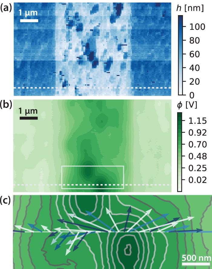
Organic field effect transistor: (a) topography, (b) electrostatic potential, and (c) electrostatic potential contours and the vector electric field along a line.
The image in (a) is an atomic force microscope image of an organic transistor. The electrodes are the tall, dark blue features on the left and right. The working material, a small-molecule organic semiconductor, is sits in the middle of (a). The image in (b) shows the electrostatic potential ϕ versus (x, y) over the transistor after it has been operated for some time and then turned off. The white square indicates a region of relatively high electrostatic potential. This high potential is due to trapped charge.
Now the cool part. The image in (c) shows lines of constant electrostatic potential near the trapped charge. In (c) we show the in-plane vector electric field E = (Ex, Ey) collected along a line (using methods introduced in the paper). We learn in freshman physics that, because the electric field is the negative gradient of the electrostatic potential, the electric field E at a location r must be perpendicular to a line tangent to the constant ϕ(x, y) surface passing through r. This perpendicular relationship is clearly evident in the experimental data shown in figure (c).
This work was funded by the U.S. National Science Foundation.